Mold fabrication — Micromachining methods
Two types of microfabrication techniques exist:
- Indirect microfabrication method which requires a master with the negative of the design of interest to mold the sign you want on your future microfluidic chip
- Direct microfabrication method which requires no intermediary and directly process the fabric you selected for your future microfluidic chip.
Among indirect microfabrication methods, many have been used in the past for the fabrication of molding tools but not all of them are suitable for microfluidics. Only micromachining methods are presented here.
Machining is any of various processes in which a piece of raw material is cut into a desired final shape and size by a controlled material-removal process. As the substrate is directly worked, it is easier to work on a silicon wafer as it can be anisotropically wet etched, forming highly regular structures, due to its crystal structure (atoms are arranged periodically and certain plains are weaker and are more inclined to be etched). Additionally, silicon offers the best characteristics with respect to cost, metallization and machinability. This type of etching is rather cheap and is generally used in early research.

Etched grooves using (a) anisotropic etchants, (b) isotropic etchants. Image source: [1]
The etching can be either isotropic or anisotropic:
- Anisotropic etching: the substrate material is attacked by etchants depending on its crystalline structure so there are different rates depending on crystallographic directions. Etchants also have the ability to control the lateral extensions of the etched profile. But etching rates are considerably lower than those of isotropic processes, thus, the masking material has to be chosen carefully as the chemical products are strong and the process can be very long. The surface roughness of the etched material can be high after this type of etching, so, for smoothing purpose, an anisotropic etching can be followed by a short isotropic etch;
- Isotropic etching: the etch rate is equal in all direction as it does not depend on the crystalline structure of the substrate. Thus it produces rounded depressions on the surface of the wafer and undercutting the masking layer on top which also makes masking a difficult task when etching isotropically. Furthermore, the concentration of acid used, the processing temperature and the grade of agitation of the sample have an influence on the etch rate. Rates of up to 50µm/min (e.g.: etch rate of SiO2 is 300 to 800 Å/min) can be achieved and are about 100 times faster than anisotropic etching.
For both isotropic and anisotropic etching, the backside of the wafer has to be protected to prevent any contact between it and the liquid. This can be done mechanically (by keeping it in a special holder) or chemically (by coating with a protection layer, e. g., waxes).
Wet etching
For wet etching process, the substrate is partially covered with a protective coat (which will not be attacked by etchant) and is generally immersed in a bath of etchant. With wet etching, both anisotropic and isotropic profiles can be achieved. The etchants differ with respect to their specifications regarding handling, toxicity, appropriate masking material and their anisotropicity or isotropicity characteristic. The etch rate depends on the etchant concentration used: the etching process is generally slowed down with high etchant concentrations, since the water in which the etchant is diluted is needed in the process as an oxidizing agent for silicon.
Advantages: fast, flexible, high quality prototyping and can achieve high volume production (e.g.: up to 50,000 wafers a year for HF etching) [2];
Drawbacks: some etchants remain very toxic and hard to handle, isotropic etching induced a special care in the choice of the geometry at nanoscale (<50nm, problems if areas to etch are to close between each other);
Common isotropic etchants: mixtures of hydrofluoric acids (HF)/nitric acid (HNO3) with either acetic acid (therefore we talk about hydrofluoric, nitric, acetic (HNA) systems) or rather water being used for dilution; buffered hydrofluoric acid (BHF).
Common anisotropic etchants:
- Hydrazine N2H4/H2O/IPA at 115ºC ー advantages: the surface quality is very good, depending on the water concentration and the temperature of the solution, SiO2 nearly as many metallic film are not attacked; disadvantages: explosive at concentrations of 50 % and above in solution with water and very toxic (carcinogenic);
- potassium hydroxide (KOH)/H2O solutions, sometimes with ispropyl alcohol (IPA) additive at 65-85°C ーadvantages: can be used in near saturated solutions at up to 80ºC;. disadvantages: can cause blindness in contact with the eyes, processing temperatures above 80°C affect the uniformity of etching and produce unwanted fumes, etch selectivity between Si and SiO2 is too low, so mask layers made of oxide are attacked quickly (additional process steps with alternative masking materials (e.g.: Si3N4) are needed). To limit high surface roughness implied by long etch times when using solutions of high concentration, the immersed sample has to be agitated; mask materials: Si3N4, SiO2 (etches at 2.8 nm/min);
- ethylene diamine pyrocatechol (EDP), diluted with water at 115ºC [3] ー organic etchant, developed to replace hydrazine. Advantages: more stable and less toxic than hydrazine, good selectivity between Si and SiO2, gold, chromium, silver, copper or silicon nitride; disadvantages: still toxic, ages fast; mask materials: SiO2, Si3N4, Au, Cr, Ag, Cu;
- tetramethyl ammmonium hydroxide (TMAH) and water at 90ºC [4] ー appropriate working concentration is approximately 22 wt% which is a reasonable compromise between surface smoothness (need more saturated solutions) and etch rate (need more water). Advantages: non-toxic, easy handling; disadvantage: lower etch rate of Si; mask materials: Si3N4, SiO2;
Dry etching [5]
Dry etching is a category of methods based on material removal reactions which occur in the gas phase. There could be either plasma based or non-plasma based techniques.
Non-plasma based technique is an isotropic (on Si) method which uses spontaneous reaction of appropriate reactive gas mixture and is highly controllable via temperature and partial pressure of reactants. It typically uses fluorine-containing gases (fluorides or interhalogens) that etch Si.
Plasma based techniques use radio frequency (RF) power to drive chemical reaction. Different type of techniques exists:
- physical etching (sputter etching): highly anisotropic, uses Argon, may result in re-deposition, etch rates for most materials are comparable;
- chemical etching;
- Reactive Ion Etching (RIE): anisotropic method, chemical etching is accompanied by ionic bombardment which leads to greatly increased etch rate and lower selectivity. But this induces conflict between high etching rate and anisotropic profile;
- Deep Reactive Ion Etching (DRIE): as it uses lower energy ions, it implies less damage and higher selectivity. It is an anisotropic etching which can achieve fast, deep, high density and high aspect ratio (1:15) structures in glass (fused silica) and silicon substrates with fine resolution.
Advantages: no dangerous acids and solvents needed, uses small amounts of chemicals, isotropic or anisotropic etch profiles, directional etching without using the crystal orientation of Si, faithfully transfer lithographically defined photoresist patterns into underlying layers, high resolution and cleanliness, less undercutting, no unintentional prolongation of etching, better process control, ease of automation (e.g., cassette loading).
Disadvantages: gases might be quite toxic and corrosive, re-deposition of non-volatile compounds, need for specialized (expensive) equipment.
Sawing, cutting, milling, turning or micro electro discharge machining [6]
Some conventional machining tools had undergone miniaturization. Thus, they are suitable for master fabrication purpose.
Advantages: wide range of materials which can be machined, only available method for machining stainless steel, good mold insert lifetimes, no mask needed and lithography step involved make development time shorter;
Drawbacks: some geometries cannot be well fabricated with these methods (high aspect ratio structures, very deep holes, channels crossings, very small structures);
Structures range: few 10µm;
Ideal geometry: simple geometry structures with straight walls;
Impossible geometries: high aspect ratio structures, very deep holes, channels crossings, very small structures.
Among these conventional methods, micro electro discharge machining, which is based on material removal due to high energy electric discharge, has a potential for further development. It allows a high degree of flexibility (materials, geometries) but master surface is comparatively rough.
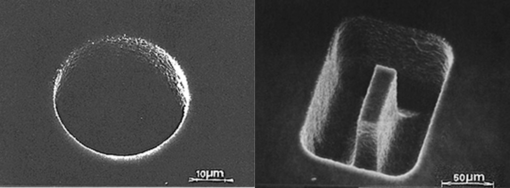
Micro electro discharge machining results in Si. Image source: [7]
References
[1] http://terpconnect.umd.edu/~sandborn/research/JPL_MEMS/microeng_bulk.html
[2] http://www.micronit.com/technologies/fabrication-technologies/etching/
[3] Finne, R.M.; Klein, D.L., A Water-Amine-Complexing Agent System for Etching Silicon, 1967, Journal of the Electrochemical Society. 114: 965–70
[4] Shikida, M.; Sato, K.; Tokoro, K.; Uchikawa, D., Surface morphology of anisotropically etched single-crystal silicon, 2000, Journal of Micromechanical Microengineering. 10: 522.
[5] J. Rossier, F. Reymond, P.E. Michel, Polymer microfluidic chips for electrochemical and biochemical analyses. 2002, Electrophoresis, 23, 858.
[6] H. Becker, C. Gärtner, Polymer microfabrication methods for microfluidic analytical applications, 2000, Electrophoresis, 21, 12-26.
[7] Lectures from Dr. T. Fetah Kosar of the Center for Nanoscale Systems, Harvard University, 2014.
For general information
For further information, do not hesitate to contact our team of experts:
contact@blackholelab.com or phone: +33(0).782.831.207