Microfabrication techniques — Photo-ablation by laser-based technologies
Two types of microfabrication techniques exist:
- Indirect microfabrication method which requires a master with the negative of the design of interest to mold the sign you want on your future microfluidic chip
- Direct microfabrication method which requires no intermediary and directly process the fabric you selected for your future microfluidic chip.
Among direct microfabrication methods, many have been used in the past for the fabrication diverse items but not all of them are suitable for microfluidics. Only laser-based methods are presented here.
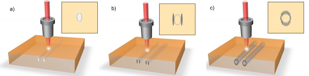
Schematic plots of the fs-laser written waveguides in crystals in diverse configurations: (a) Type I: direct-write waveguide (b) Type II: stress induced waveguide, and (c) Type III: depressed cladding waveguide. The insets show the cross sectional plots of the waveguide endfacet. The dashed lines indicate the spatial location of the guiding core in respective geometries – Image source
General principle and advantages [1]
The laser processing technique is based on a contactless process which does not require a clean-room: laser ablation. The laser energy can be concentrated on microscopic areas and can lead to a partial material removal according to several parameters that maximize the absorption of laser photons by the sample material on defined parts of it:
- material: any material can be laser machined (ceramics, metals, polymers,…) and a process with a new material is rather easier to develop with laser ablation processing than with other processes. The use of ultrafast lasers (e. g.: femtosecond lasers) may enable the machining of materials normally transparent to the laser wavelength.
- pulse duration: from microseconds to femtoseconds
- wavelength: deep UV (157µm) to IR (10µm)
The broad panel of laser sources enables to process very different kind of materials at different prices: as the field is developing rapidly, it is easier now to found less expensive laser micromachining devices. The use of lasers could also enable to handle some materials differently: concerning PDMS devices, features can be fabricated in pre-cured polymer which can prevent from some dimensional changes due to curing.
It has to be noted that laser ablation is also able to significantly change the surface properties (wetting properties, surface charge, formation of new functional groups,…) of the substrate without damaging the surface itself.
The use of lasers in micromachining or general production is neither new nor obsolete: laser micromachining is an efficient, highly precise and flexible tool in many production areas and appears as a tool of choice in microengineering [2] thanks to its high peak intensity, spatial coherences, spectral purity and temporal coherence. Laser processing method enables to deal with non-planar substrates and complex geometries (3D shapes, different wall shapes, etch depths and aspect ratio on the same sample) by shaping substrates both laterally and into the depth of the material and that gives laser processing method important benefits over other more usual micromachining techniques.
It is possible to use laser micromachining with a mask by using parallel mode which is a technique more suitable for large-scale production. For fast prototyping, it is better to use the other mode which uses a focused laser: serial mode. This mode enables to directly “write” on the material of interest without any mask by only using data from a file to generate a path for the laser beam, enabling fast upturn. Laser machining technology can also be combined with other micromachining techniques (lithography, plasma etching, electro-discharge machining and ultra-precision milling) through hybrid processing to slower production techniques for example (e.g.: hot embossing).
Different types of lasers for micromachining microfluidic devices [1]
UV lasers
If glass micromachining still presents challenges, flexibility, modification of surface properties and fast fabrication of UV laser ablation can bring interesting assets to polymer microfabrication for microfluidics.
Several research teams used UV laser processing technique to pattern microchannels with direct laser ablation and modify the resulting surface, particularly with devices made out of polymers. The increase in the surface roughness induced by the laser ablation have been highlighted several times, especially the dependence on the laser fluence.
Associated research:
- fabrication of micrometer-sized-features channels and high aspect ratios in a variety of polymers (polystyrene, polycarbonate, cellulose acetate, and PET) using a laser at the wavelength of 193 nm [3].
- fabrication of microfluidic chips is performed in a dynamic instead of static mode, implying motion of the polymer target relative to the laser beam [4].
- a team has demonstrated the possibility of controlling the surface modification in a microchannel by alternating dynamic and static ablation procedures. They also proved that well-defined static patterning could be solution to locally modify the surface potential without using photochemical treatments [5].
Femtosecond or ultra-short-pulse lasers
Ultra-short-pulse lasers can modify substrates at wavelengths at which they are normally transparent which makes it a unique processing tool. This category of lasers provides very precise (10nm) 3D-localized machining inside the sample without affecting the rest of the target. The drilling of high-aspect-ratio capillaries is a key application of ultra-short-pulse lasers but the removal of resulting debris is a challenge. Laser-assisted microfabrication has shown that good wall-surface quality was accomplished and that low-viscosity liquids were advantageous for effective expulsion of glass debris [6].
Associated research:
- femtosecond lasers have been used with glass substrates:
- direct writing on silica glass: by combining laser machining with chemical etching (hydrofluoric acid (HF) solution), 10µm interconnected channels have been fabricated [7]. It has also been demonstrated that, without any other fabrication techniques, straight and square-wave-shaped holes could be drilled in silica glass [8].
- Foturan glass (near-IR wavelength): combined with thermal treatment and HF chemical etching, microchannels have been produced. Laser machining enables to obtain high precision and uniformity [9], as well as 3D hollow microstructures [10] inside the glass.
- for the optical analysis of reactants, microfluidic lasers and other microoptical components have been fabricated in a microfluidic device [11]
- PDMS has been directly written with femtosecond lasers (Ti:sapphire laser) and addition of functionalities (e.g.: including grooves that promotes mixing of liquids) has been performed [12]
- combined with soft lithography, ultra-short-pulse lasers enabled to add unmoldable features (microcapillaries with a diameter of 0.5µm, high aspect ratio structures – 800:1) to microfluidic devices [13].
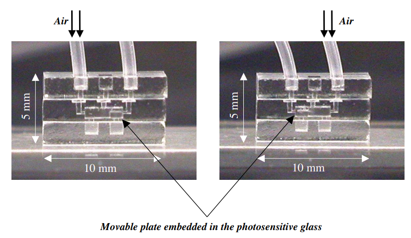
Prototype of a microfluidic device with a freely movable microplate which can switch the flow direction of reagents – Image source: [10]

(A) Single segment of a straight microchannel fabricated on a copolyester chip with CO2 laser marker. (B) Co-polyester substrate fabricated with a serpent channel using CO2 laser marker. The channel width in parts A and B is 324µm. The channel bottoms have been dyed with ink to improve visualization – Image source: [17]
Infrared (IR) laser micromachining
IR radiations have wavelengths between around 1 mm and 750 nm [14]. CO2 lasers are very commonly used as IR laser source centered around 10µm and represent a cost effective alternative to UV lasers.
Unlike UV lasers, IR laser machining is a purely thermal process: the laser beam directly applies heat on the material which partially evaporates. If IR lasers are very common in industrial applications as they are available at moderate prices, they are also suitable for prototyping polymer microfluidic chips thanks to their flexibility and speed of process. For instance, very good results of micromachining (down to 85µm-wide channels, up to 2µm concerning the smoothness of the wall surfaces) have been obtained with PMMA (high absorbance in IR, clean structures due to the thermal decomposition of the polymer) [15].
Associated research:
- polycarbonate: with CO2 lasers, low-cost and disposable polycarbonate devices have been created. They integrate several functions among which PCR and hybridization can be found [16].
- Vivak co-polyester chips: a low power process in a nearly anaerobic environment was developed. The typical fabricated feature had an aspect ratio from 0.5 to 2 and was around 350-μm wide. 2D microchannels were easily fabricated at moderate yield of approximately tens of chips per day so the production scale and initial cost fit the demand of a bioanalytical laboratory [17].
- stainless steel (Nd:YAG laser – 1,064 nm): multilayer microfluidic devices with channels down to 50 μm were fabricated [18].
Visible lasers
Copper vapour laser is a common type of laser with visible light source. Several components for microfluidics in different material (polypropylene, borosilicate glass,… [19]) were produced by using this technique. Among them, tungsten and stainless steel micro-reservoir pins have been fabricated with this laser (511 nm and 578 nm) in order to perform high-throughput screening and gene analysis [20]. It has been proved that this technique is faster (10 to 20 times more), more flexible and with a better resolution than electro-discharge machining (EDM).
When the substrate of choice is made out of silicon, 3D structured cas ben produced with visible lasers. A potential for MEMS fabrication has also been highlighted as prototypes of microfluidics components with sub-micrometer resolution have been fabricated [21].
Advantages of laser-based techniques for microfluidic applications [1]
Post processing of microstructures is a key issue of microfabrication and might be difficult to handle. Laser micromachining techniques have the advantages to be very flexible and to be easily integrated in a process to propose integrated solutions for manufacturing.
Microfluidic devices are more and more complex and so is the integration of other elements (optical, chemical, electrical,…) to the devices. That makes microfluidic systems even more functional with different levels and made out of different materials which requires flexibility and precision for the microfabrication technique, some criteria that are gathered with laser treatments.
As both surface modification (with little damage) and microfabrication are possible with laser micromachining, this technique offers numerous assets over other methods (both chemical and physical ones). Moreover, laser-based techniques are rather simple, easy to control, safe and clean for the environment.
References
[1] Chantal G. Khan Malek, Laser processing for bio-microfluidics applications, 2006, Anal Bioanal Chem 385: 1351–1361.
[2] A. S. Holmes, Laser processes for MEMS manufacture, 2002. Second International Symposium on Laser Precision Microfabrication, RIKEN Rev 43:63–69.
[3] M. A. Roberts, J. S. Rossier, P. Bercier, H. Girault, UV laser machined polymer substrates for the development of microdiagnostic systems, 1997, Anal Chem 69:2035–2042.
[4] J. S. Rossier, P. Bercier, A. Schwarz, S. Loridant, H. H. Girault, Topography, crystallinity and wettability of photo ablated PET surfaces, 1999, Langmuir 15:5173–5178.
[5] F. Bianchi, Y. Chevelot, H. J. Mathieu, H. H. Girault, Photomodification of polymer microchannels induced by static and dynamic excimer ablation: effect on the electroosmotic flow, 2001, Anal Chem 73:3845–3853.
[6] D. J. Hwang, T. Y. Choi, C. P. Grigoropoulos, Liquid-assisted femtosecond laser drilling of straight and three-dimensional microchannels in glass, 2004, Appl Phys A 79:605–612.
[7] A. Marcinkevicius, S. Juodkazis, V. Mizeikis, M. Watanabe, S. Matsuo, J. Nishii, H. Misawa, Fabrication of 3D interconnected network of microchannels inside silica by femtosecond irradiation and etching, 2001, Proc SPIE 4274:469–477.
[8] Y. Jiang, K. Itoh, W. Watanabe, K. Yamada, D. Kuroda, J. Nishii, Y. Jiang, Three-dimensional hole drilling of silica glass from the rear surface with femtosecond laser pulses, 2001, Opt Lett 26(23):1912–1914.
[9] Y. Cheng, K. Sugioka, M. Masuda, K. Toyoda, M. Kawachi, K. Shihoyama, K. Midorikawa, 3D microstructuring inside Foturan glass by femtosecond laser, 2003, RIKEN Rev N° 50:101–106.
[10] K. Sugioka, Y. Cheng, M. Masuda, K. Midorikawa, K. Shihoyama, Fabrication of microreactors in photostructurable glass by 3D femtosecond laser direct write, 2004, Proc SPIE 5339:205–213.
[11] K. Sugioka, Y. Cheng, K. Midorikawa, Three-dimensional micromachining of glass using femtosecond laser for lab-on-a-chip device manufacture, 2005, Appl Physics A 81:1–10.
[12] D. B. Wolfe, J. B. Ashcom, J. C. Hwang, C. B. Schaffer, E. Mazur, G. M. Whitesides, Customization of poly(dimethylsiloxane) stamps by micromachining using a femtosecond-pulsed laser, 2003, Adv Mater 15(1):62– 65.
[13] T. N. Kim, K. Campbell, A. Groisman, D. Kleinfeld, C. B. Schaffer, Femtosecond laser-drilled capillary integrated into a microfluidic device, 2005, Appl Phys Lett 86:201106-1–201106-3.
[14] https://www.optotronics.com/ir-lasers.php (consulted – October 4th 2017)
[15] H. Klank, J. P. Kutter, O. Geschke, CO2 laser micromachining and back-end processing for rapid production of PMMA-based microfluidic systems, 2002, Lab On A Chip 2(4):242–247.
[16] Y. Liu, C. B. Rauch, R. L. Stevens, R. Lenigk, J. Yang, D. B. Rhine, P. Grozinski, DNA amplification and hybridization assays in integrated plastic monolithic devices, 2002, Anal Chem 74:3063–3070.
[17] S. C. Wang, C. Y. Lee, H. P. Chen, Thermoplastic microchannel fabrication using carbon dioxide laser ablation, 2005, J Chromatogr A 1111(2):252–257.
[18] J. Lichtenberg, H. Baltes, Lowcost, chemically resistant microreactors fabricated by laser micromachining in stainless steel, 2004, Proc 8th int conf on miniaturized systems for chemistry and life sciences, Sept 26–30, Malmö, Sweden, pp 351–353.
[19] E. Illy, G. Rutherford, A. Bell, M. Knowles, Laser processing of microfluidic components and bioMEMS, 2003, Proc SPIE 4982:130–137.
[20] S. Elmes, J. Pearson, D. F. Moore, G. A. Rutterford, A. I. Bell, N. Rivara, M. H. R. Knowles, Laser machining of micro reservoir pins for gene analysis and high-throughput screening, 2001, Proc laser microfabrication conf (ICALEO), Florida, USA, 15–18 Oct 2001, pp 1–10.
[21] M. Müllenborn, H. Dirac H, J. W. Petersen, S. Bouwstra, Fast 3D laser micromachining of silicon for micromechanical and microfluidic applications, 1995, Proc IEEETransducers 95 – Eurosensors IX, pp 166–169.
For general information
For further information, do not hesitate to contact our team of experts:
contact@blackholelab.com or phone: +33(0).782.831.207