Lamination of dry film to create microfluidic chips!
What is dry film lamination?
 The dry film lamination process consists in deposit a dry film of photoresist on a substrate thanks to two rotating rolls pressed against each other. Different parameters can be adjusted such as the temperature rolls, the speed of the lamination and the pressure between the rolls. The dry film lamination replace the spin coating when working with liquid photoresist.
The main advantage of such option is to save time because you work directly with the film thickness you desire not need to spent time making it, preventing especially the long baking time that can occurs working with liquid photoresist such as SU8. What’s more the fry film process is far more cleaner than the spin coating one and you will save a lot of cleaning time. On the opposite your are limited in the thickness choice. An other limitation of the dry film lamination will be the minimum thickness achievable, indeed the smallest commercial films are around 5µm and are not widespread, instead the liquid spin coating can go down to hundreds of nm.
Of course lamination processes can be used for other application such as, the bounding of two heat-sensitive materials or be an equivalent of the hot embossing, but only the use of photoresist film will be discuss here.
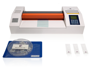
If you are interested by working with dry film lamination, please have a look at our Dry film lamination station!
The choice of the dry film
There is only two choice to get your dry film: you can by it or you can make it. For each solution there are some advantages and drawbacks that we are going to see here.
Commercial photoresist dry film:
It exist different kind of commercial dry film with different chemical, mechanical, physical properties. Some can be permeant photoresist like the SU-8, or easily removable so the choice of the film depends on the right application. A commercial film is always almost presented in the same way with a triple layers film, composed of the photoresist and on both side a protection plastic film.
There are two relevant advantages of using a commercial film, first the film is already done so you save time to not making it and then the thickness is already defined with a really good uniformity over the film. The other advantage is regarding the price, indeed for equivalent surface coated, the dry film are often cheaper than liquid photoresist. However this statement have to be balanced, because the minimum quantity of dry film that you can bought are high and the investment represent quite the same than with liquid photoresist.
The dry films are quite stable in time but need to be keep off the light and humidity. Well packed it can be store in a fridge if not use for a while. The advise limit of use will be often one year, however it’s still possible to use it after but you might loose some resolution possibilities during the process.
Make you own dry film:
It is also possible to fabricate yourself your photoresist dry film in SU-8 for example. To do such a thing, you need to put your resist on a plastic film with a classical spin coating process for example. Be careful the choice of the film is really crucial, indeed, depends on the wetability between the film and the photoresist, the layer can stick to the film after transfer (if the photoresist wet too much the plastic film) or the photoresist can’t be well spread on the film (if the photoresist doesn’t wet enough the plastic film). For exemple, for the SU-8 photoresist an angle contact really close to 80° enables a good coating of the photoresist on the substrate and the layer will be correctly transfer on your substrate during the lamination step.
This option of making your own dry film allow you to be free in the thickness but of course you keep all the drawbacks of liquid photoresist (mainly time consuming and dirty process). In the other hand you can add components to your film by mixing it at the liquid base.
What you can do with dry film lamination?
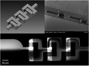
Mold for softlithography
 One of the first obvious application is simply the creation of mold for softlithography process. It’s what we saw before, the lamination process replacing the spin coating one working with dry film instead of liquid photoresist. The height of the mold will be the thickness of the film or a multiple. Indeed it’s possible to laminate a new film on a first one and to repeat this step almost as many time as wanted. (You have to keep in mind that more lamination process you do and more chance you have to create defects so at the end there is a limitation). And so it appears that for thick layer the lamination process is better and easier.
Because of the different material of dry film, all the mold won’t have the same chemical or physical resistance, and compare to the well-known SU8 mold, some may be break after a first polymer replication. Which can be painful if the mold need to be done for each chip fabrication. But in this case it’s possible to duplicate the alone polymer chip on an epoxy mold to make more again later.
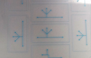
3D microfluidic devices
 Thanks to the lamination technique, it is also possible to directly create your microflduidic devices which will be entirely in photoresist.
Indeed, it’s possible to pattern a first layer with channels and then to laminate a new film on the top to close the channels. At this step you have fully close channel but it’s possible to expose this new layer to make holes to connect the lower channel to the top. Of course this part need the capability to align during the exposure step. When you have done this for a two layer device you can repeat this several time also and so create complete 3D structures directly in your dry film photoresist.
This option enables to have solid devices compare to the soft PDMS.
For general information
For further information, do not hesitate to contact our team of experts:
contact@blackholelab.com or phone: +33(0).782.831.207